At the Chemnitz University of Technology we use to teach the computer science students how to program in assembly language (i.e. how to program processors directly). As exemplary processor-target the wide spreaded 80×86 architecture was used. Of course, the primary reason for this target was the fact that development host and the test system are the same.
Over the years the software has evolved and you cannot leave the students working with some outdated technology such as DOS. Instead, they start asking you: “Hey, with what kind of antiquated tools we are forced to work here?” As a result, their interest in the matter is reduced significantly. This is not true for all students, but for the broad mass.
Now one would ask why it is not possible to write assembly programs in the framework of modern operating systems such as Linux or Windows. Of course, it is well possible. But these operating systems restict the use of several important features due to safety reasons. This is especially true for IO related stuff (interrupts etc.).
So the decision has been made to switch at least partly to a micro controller based system where one has total control
Of course, there are also other options to cope with the limitations. Virtual machines or even complete simulators are an example. However, working with a real hardware is much more fun. Also, the students can identify themself much better with a small piece of hardware rather than with a big complicated system. And the more fun, the better the learning curve. Additionally, the field of micro controllers became extremely important during the last years.
Because there were no suitable evaluation boards available, we decided to built one by ourself. So it was finally my task to do this while I got some help from Ralph Schlosser, a student in Chemnitz.
Basic Hardware:
The training board is based on an 8051 derivate from Cypress (AN2131SC). This MCU has an integrated USB interface that can also be used to load programs into the system. This makes it quite easy and simple to use. The USB interface is actually not just a simple interface. It plays a key role in the MCU as it can take full control on the actual micro controller.
Here’s a list of some AN2131SC features:
- 256 bytes internal RAM (part of 8051)
- around 8kB RAM for code and external data
- 18 digital IO lines
- complex USB interface
- 2 UARTs
- 3 Timers
- 24MHz clock (4 clocks per instruction cycle)
For more information refer to the manufacturer’s web site:
http://www.cypress.com/products/datasheet.cfm?partnum=AN2131SC
Software:
The used development software is running under Linux.
First of all there is an appropriate USB-driver (kernel module) needed. A free one that has been written by Tony Cureington is available here:
http://ezusb2131.sourceforge.net
A small free assembler (as31) has been written by Ken Stauffer and it can be downloaded from here:
http://www.pjrc.com/tech/8051/
IO-Stuff implemented on the Board:
The training board contains the following components:
- two simple LEDs (a red and a green one)
- two passively debounced buttons, that can also be used to trigger interrupts
- two 7-Segment displays that need to be driven in a time-multiplex fashion in order to display two different values
- a piezo-ceramic sonic converter (can also be controlled via timer output which simplifies the handling significantly)
- a standard RS232 serial interface (RxD and TxD) primarily intended for some kind of serial console
- USB interface, of course primarily for uploading programs and to provide power
- 8kB serial EEPROM that can be used to store a program in the case of autonomous (without USB) operation
Some Pictures:
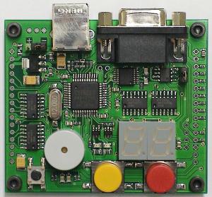
The following picture is a view from above the board.

Most of the aforementioned components are clearly visible. The bigger chip in the middle is the AN2131SC micro controller.
The two ICs at the left side of the board are a standard logic D-FlipFlop (74HCT74) and NANDs (74HCT00). Both are related to the buzzer handling.
Below the standard 9Pin SUB-D connector for the serial port is the RS232 level converter (left) and the serial EEPROM (right) visible.
Above the 7-Segment displays two standard logic inverter ICs (74HCT04) can be found. They are needed for the control of the displays. Besides the inverter functionality, they convert 3.3V logic levels to 5V logic levels that are needed for the blue LEDs.
A small reset button can also be found bottom-left.
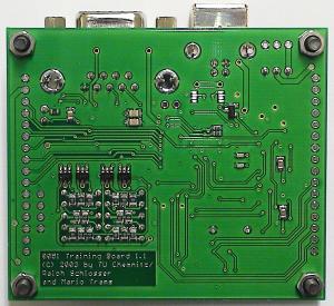
At the left and the right side the board is prepared for taking up expansion connectors. Almost all signals of the MCU are available there and might be used for other applications. The bottom side is looking as following.

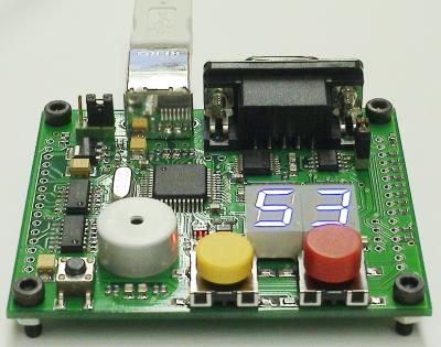
There’s not much to say here. The circuitry in the lower-left area can be called the end-stage for the 7-Segment displays. These are a few (four dual) MOSFETs and current-limiting resistors. Finally, a perspective view showing the board in action.

Contact
If you are interested in more details, just send me an Email: Mario.Trams@digital-force.net