This project (in the following text referred as PowerMonitor) was initially targeted to serve as a measurement tool for 12V/24V electrical power systems in harsh environments. In particular for an off shore sailing yacht where it was and is intended to act as some kind of multimeter for some electrical power buses. There it is being used to watch over various voltages and currents that are involved in a system consisting of multiple batteries, generators, and photovoltaic solar panels.
Meanwhile, this system is serving its duty within the target application very well.
Basic Requirements:
Here are a few of the basic requirements for the PowerMonitor:
- Direct power supply from 12V or 24V raw power rail
That is, the PowerMonitor can be directly attached to a more or less unregulated and unstable power bus. This also means that it must survive intermediate voltage spikes of up to 60V. Such high voltages are typically assumed for automotive systems that include generators and motors.
In the end, the PowerMonitor can be supplied from a wide input range of 7V-42V DC. - Distributed measurement capability
The PowerMonitor needs to be able to measure voltages and currents directly at various critical locations.
Due to the accuracy of the measurements it is not possible to just feed some wires to a central unit that is finally carrying out the measurements. So the overall design has been laid out so that it is consisting of so-called Measurement Units carrying out the actual measurements very close to the area of interest by means of performing the needed analog-to-digital conversion. The digitized voltage and current samples are sent digitally to a Central Unit where they are processed further.
The final system supports up to four Measurement Units, where each one is capable to measure one voltage and two currents. Each Measurement Unit can be attached to a different electrical circuit and the two current and one voltage channel share a single reference, which is typically the plus pole of a battery. - Very accurate and wide range of high-side current measurement capability
Well, what does “very accurate and wide range” mean? Wide range means that currents into the hundreds of Amperes need to be measured. But at the same time it shall be possible to measure currents in the range of Milliamperes. In fact, the nominally achieved current measurement resolution is 3-4mA assuming an 100A/60mV shunt.
“high-side” means that the currents are to be measured at the plus pole of the according system rather than in the ground path. This is the preferred way for measurements involving batteries where you are interested in the currents flowing into and from various other systems. However, precise high-side current measurements cause additional complexities, especially when higher voltages are involved. - Also very accurate voltage measurement capability in the interested range
The voltage measurement is not that difficult as the current measurement. It has been laid out to formally work at a nominal resolution of 5mv (10mV was the requirement) and is working across a range of +/-160V (DC, of course). Although this is unnecessarily high, this has been chosen in order to be able to have a rather high protection level of the voltage measurement channel to survive even higher discharges or whatever.
It needs to be mentioned that in the configuration that has been finally chosen the voltage measurement is slowly becoming inaccurate when the input voltage is between -5V and +5V or so. However, this is not an issue, as the nominal system voltage is usually around at least 12V. - Low power design
Low power consumption is always an issue, especially in self-sufficient systems.
Implementation Details:
The System is consisting of
- A Central Unit Main Board
This board is containing the primary processing hardware and firmware.
Up to four measurement units can be attached to the main board. - A Central Unit IO Board
This is a supplemental board that is being hooked up to the main board and just contains a LC display and a few buttons - The Measurement Units
Those are more or less identical units that are located directly at the position where the measurements are to be carried out.
Central Unit Main Board
The following picture is showing a photograph of the primary side of the main board.
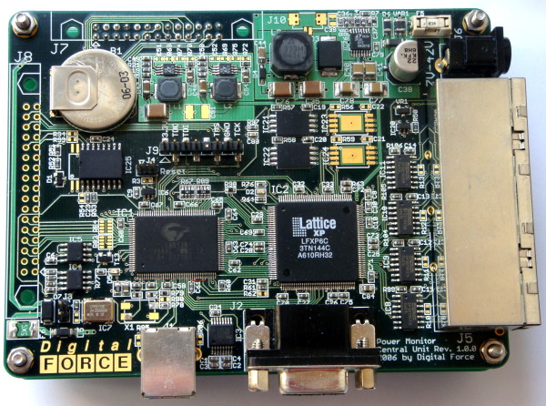
Here are a few facts about the main board:
- The board is a 4-layer board and is 12cm by 9cm in size.
- As processor the 8051 that is integrated within a Cypress FX2LP USB Controller has been selected (above the USB connector). This decision has been made because the USB connection seemed useful for reading back logged measurement data (never implemented, actually….) and it was also quite convenient and simple in view of the firmware development. Last but not least the FX2LP was a well-known device, which is also an important factor. The firmware has been implemented in C (partially assembly language) using SDCC. However, as it turned out, this processor is hardly at its limit for this application. Not because of its calculation power, but because of its limited memory resources.
This processor is also running a tiny multi-threading like task scheduler that has been specifically developed for this project. More detailed information about the task scheduler is available on a dedicated project page (An Ultra Small Real Time Multi Tasking Kernel for Embedded Applications). - The firmware code as well as other vital configuration information and some logging information is stored within I2C EEPROMs located left to the FX2LP.
- At the upper/left area a real time clock and an associated backup battery can be seen. The RTC is a Maxim (formerly Dallas) DS3231 very high precision RTC. The battery is a Lithium Mangan Dioxide rechargeable one which will become automatically charged when the system is being powered up. It should keep the RTC running for about 2 years without turning the PowerMonitor on.
The primary purpose of this RTC was for accurate time-stamping of logged measurement data. However, that has never been implemented. So the RTC is just acting as a precision timekeeper now…. - At the upper area there are some switching power regulators. Specifically important is the main input regulator which one is deriving 6V from the unregulated input power supply. A Linear Technology LT3435 is being used here. The remaining two regulators generate 1.8V resp. 3.3V for various devices.
- The Lattice Chip (LFXP6C) is an FPGA that is containing vital logic resources especially for the packet communication with the measurement units. It does also provide some additional RAM to the 8051. Furthermore it allows the 8051 to communicate with some SPI NOR Flash EEPROMs that are located above the FPGA.
- The NOR Flash EEPROMs are M25Pxxx types from ST Microelectronics (now Numonyx). Only two of them are soldered on the board shown on the photograph. Initially they were intended to log measurement data for a later analysis. However, that has never been implemented, and doing so at the level of interest seems not possible with the 8051.
- To the right the connector for the measurement units is visible, and left to this connector the RS485 transceivers for the electrical communication level. For simplicity, an RJ45 connector system has been used. The electrical connection to the measurement units is being equipped with some automatic detection mechanism as well as with an electronic fuse mechanism in order to automatically turn off a measurement unit in case an unusual over-current has been detected. This mechanism has been tested by just shortcutting the power supply of a measurement unit – outch! 😉 – and is working well.
- The connectors at the bottom provide a standard RS232 serial interface (that has never been used so far) and the USB connection. As previously mentioned, one of the primary purposes of the USB connection was to be able to read back logged measurement data into a regular computer (notebook etc.) for analysis purposes. However, this has never been implemented. So far, there has been just defined some protocol to allow an in-field firmware update (I2C EEPROM access) via USB.
- The Connector at the top/left (mounted on the reverse side) is the connector for the IO board for interfacing with the display and the buttons.
- On the left edge of the board there is visible a provision for another connector where some additional hardware might be attached – who knows…. 😉
Central Unit IO Board
The following picture is showing the most interesting side of the IO board.
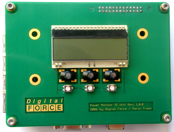
Here are a few facts about the IO board:
- The board is also 12cm x 9cm wide but has just 2 layers.
- The main part of the board is a DOGM LC display from Electronic Assembly with 2×16 characters.
- Below the LC display there are located three so-called “optical buttons” that have been implemented for the very first time there. So to speak, this is the first official reference implementation of this button concept. More details on these buttons can be found on the dedicated optical button project page.
- On the reverse side of the board are mostly just some analog components needed for the optical buttons.
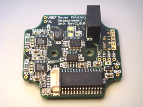
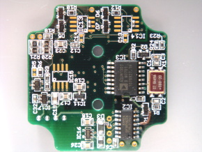
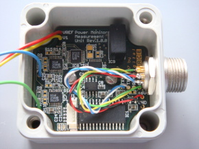
A single measurement unit is intended to measure two high-side currents and one voltage within a single electrical circuit. The topology of the measurement setup is made in a way, where a common measurement wire is being attached to the plus pole of the battery, the voltage measurement wire is being attached to the minus pole of the battery, and two current measurement wires are attached to the two shunt resistors located at the plus pole of the battery. Notice that this setup does contain a small flaw (see further down).
The measurement units are basically self-contained small embedded systems. Here are a few comments:
- The board is a multilayer board with 4 layers and an overall dimension of 44mm by 42mmm which has been specially designed to fit in a Bopla housing that has been found useful for this application (see photographs).
- From point of view of their basic architecture, they are very similar to the Plane Sensor for Inertial Measurement. In fact, the micro controller firmware and the communication infrastructure is significantly based on this technology.
- The communication between a measurement unit and the central unit is based on a robust RS485/422 electrical level and does also include some forward error correction for the transmitted data.
- The heart is formed by a PIC16LF76 micro controller.
- The analog-to-digital conversion is being done by three independent Analog Devices AD7792 16 Bit Sigma-Delta converters. Two for the current channels and one for the voltage channel. The AD converters are set up to deliver samples at a rate of 10Hz which is ok for that application (it could also be set to a higher rate).
- The analog-to-digital converters are galvanically isolated from the micro controller and hence the remaining PowerMonitor. This is an important requirement for the special current measurement technology that has been implemented here (see further below).
The galvanic isolation is not realized by opto couplers, but by so called iCouplers from Analog Devices. These state-of-the-art isolation devices are more reliable and consume less power. - The power supply for the analog-to-digital converters is realized with a galvanically isolated DC-DC converter. In particular, a C&D Technologies LME0505SC (5V/5V) has been used. Although this does not seem to be the best solution because this device does formally consume almost half of the power needed by a whole measurement unit, it has been chosen for the sake of simplicity, as there was no experience with building up such a specialized device in a much more efficient manner.
- For the connection of the measurement unit to the central unit a rather expensive and hermetically sealed and water-proof connector from Tajimi Electronics has been chosen. Together with the hermetically sealed housing, the measurement units can also operate in a flooded environment, if needed – hopefully not 😉 The four measurement cables that can be seen in one of the pictures are also being fed out of the housing so that it remains sealed.
PowerMonitor at work
The following picture, despite of somewhat poor quality, is showing the PowerMonitor at work in its final application including a simple front panel.
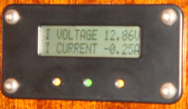
In the moment shown, its operational state is in the so-called “interactive mode” where the yellow buttons can be used for walking through the measurement channels for the top respectively bottom line. The middle (green) button can be used for entering a menue where various settings and adjustments can be made.
As it can be seen, because of the limited display capabilities only two measurement channels can be visualized at once.
Employed Current Measurement Technology:
There need to be added a few more words regarding the methodology of the current measurement.
The defacto-standard for doing this is by using precisely trimmed shunt resistors that are placed into the current path. The voltage appearing across the shunt is proportional to the current flowing through it (just following Ohm’s Law) and can be measured rather easily.
However, shunt resistors are per definition uncool and completely unsexy especially when talking about high-power electrical systems. They get warm at higher currents and hence energy is being wasted. Some voltage is being dropped too.
As a possible alternative there has been evaluated another current sensing technology based on hall-effect sensors. Allegro Microsystems is offering several devices that seemed quite promising. Another advantage of this technology is the inherent galvanic isolation from the electrical circuit that is under measurement.
However, as it turned out, these devices cannot (yet) be used for systems that require a wide range into the hundreds of amperes while still allowing a precise measurement of a few milliamperes. Therefore this had to be dropped, unfortunately. But I’m sure that this technology will be pushed as well and will be improved over the next years.
Another similar technology are so-called current transducers. This is an older technology that even allows to measure the current flowing through a cable without the need to open/cut this cable. This is an almost optimal solution. However, there have been made no in-detail evaluations here, because these devices seem to require a lot of energy to operate and are more likely suitable for even higher power-class applications that also do not require a precise measurement in the range of milliamperes.
So finally the bitter pill had to be taken and the shunt solution has been implemented. But here was another challenge regarding the requirement for a high-side current measurement in junction with potentially up to 60V of input voltages. While this is a well-known problem, the industry is providing special amplifiers for dealing with shunt measurements by offering a so-called common-mode input range of up to 60V. However, these devices do have a significant drawback: They are by the order of a magnitude less precise than their counterparts that are not suitable for such a high common-mode input voltage.
In order to deal with that issue a very simple but effective method has been introduced: A galvanically isolated power supply is being generated that will be connected to the electrical circuit that is to be measured. This power supply can be also derived from the circuit to be measured, of course. Then the ground of this “new” power supply can be attached to the high-side shunt and all high-voltage common-mode problems disappear like magic. Hence ultra-precise operational amplifiers can be used in the path for measuring the voltage across the shunt. In this particular case, the shunt from the more or less rough environment is being directly connected to the very fragile and ultra-precise AD converter without any additional buffering.
There is also planned the preparation of a white paper that is describing this technology in more detail.
Future Work:
This project is basically done and is already working fine in the targeted application. However, as usual there are many things that could be improved. Here are a few of them:
- Complete Objective Performance Analysis
Of course, the data delivered by the PowerMonitor has been checked against a regular multimeter for its correctness. Do not ask for the exact precision that has been finally achieved, as it as not been written down that time 🙁 But the tests – especially the current measurement tests – have not been made with tons of Amperes, as this is not trivial…. So it would be interesting to know what the PowerMonitor can achieve over its full formal capabilities. - Improvement of the Display Capabilities
Instead of the rather poor LC display that is being currently used, some larger one could be used. Possibly some OLED/PLED or TFT screen. This would allow a more extensive and more “verbose” and intuitive display. - Implementation of Logging Capabilities
It would be really interesting to log or trace the measurements over a longer time (hours, days, months, ….) in order to have the capability for a later analysis of the power system and its possible optimization. - Environmental Hardening of the Central Unit
Although the central unit is usually not exposed to the rough environment as the measurement units are, it could be made mechanically more bullet-proof and also more (or at all) hermetically sealed. - General Re-Make of the Central Unit
In view of enhancements such as logging and better display capabilities it seems to be sensible to migrate to another processor or micro controller system with more capabilities – possibly running Linux or uCLinux. - Improvement of the Measurement Unit
The measurement unit could be improved by throwing away the currently used DC/DC converter and replacing it with a solution specifically designed for this application. The currently used converter has a rather high power consumption of 10mA which is very likely caused by its cheap design. Currently, a complete measurement unit is drawing somewhat over 20mA @ 6V. So this is a significant contributor.
Furthermore, the measurement unit is containing a minor design flaw as it is sharing a single measurement cable for the two shunts of the two current measurement channels. This is, however, not good practice because attaching the measurement cables to shunts is usually a critical matter. Every microvolt is counting there. And, in fact there have been observed minor current measurement anomalies because of this flaw when both channels are being used. This issue could be solved by providing two independent power supplies – one for each shunt. Alternatively, two measurement units can be used instead of just one, or the minor error is being tolerated (as it is done currently).
For comments or questions you can contact me by email.